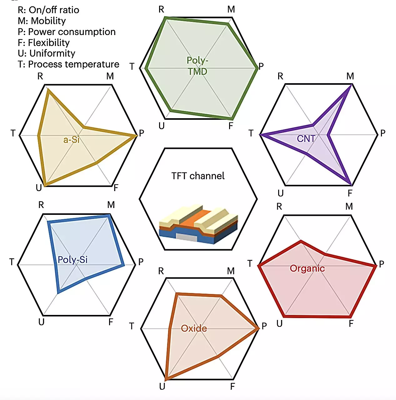
The field of electronics engineering has been continuously evolving, with a particular focus on designing smaller and more advanced transistors. Traditional silicon-based field effect transistors (FETs) have certain limitations when it comes to scalability, prompting researchers to explore alternative materials with higher electron mobility. Transition metal dichalcogenides (TMDs) have emerged as one of the most promising materials for the development of scalable FETs, thanks to their small length and excellent carrier mobility. Among these materials, molybdenum disulfide (MoS2) has generated significant interest due to its unique properties.
A groundbreaking study conducted by researchers at Samsung Advanced Institute of Technology (SAIT) and Seoul National University showcased the integration of MoS2 transistors on a 200 mm wafer. This achievement was documented in a paper published in Nature Electronics, highlighting the scalability of MoS2 transistors and their potential for creating smaller and more flexible devices. The researchers emphasized the importance of two-dimensional semiconductors like MoS2, citing their scalability, transferability, atomic thickness, and high carrier mobility as key advantages for thin-film transistor applications.
The research team utilized a technique called metal-organic chemical vapor deposition (MOCVD) to fabricate large-scale arrays of MoS2 FETs. By successfully eliminating the Schottky barrier between the MoS2 material and metal, they were able to enhance the carrier mobility of the transistors. The fabrication strategy employed was compatible with existing electronic manufacturing processes, with a remarkable yield of over 99.9%. The team’s innovative approach to redesigning the process flow resulted in MoS2 FETs with mobilities of 21 cm2 V-1 s-1, contact resistances of 3.8 kΩ·μm, and on-current densities of 120 µA μm-1.
The FETs developed by the research team demonstrated exceptional performance in initial tests, surpassing previously introduced MoS2-based FETs in terms of field-effect mobility, contact resistance, and on-current densities. The team attributed this success to the elimination of the Schottky barrier at the MoS2/metal interface and the reduction of contact resistance through new fabrication steps. Additionally, they identified key factors that contributed to the superior performance and yield of their devices, including the absence of impurities on the contact and prevention of material peeling off. Integration of the FETs on a 200 mm wafer revealed uniformity with minimal die-to-die variations, showcasing the potential for large-scale commercial production.
Fueling Innovation and Commercialization
The research conducted by the team at SAIT and Seoul National University opens up new possibilities for the electronics industry. By demonstrating the feasibility of integrating MoS2 transistors on a 200 mm wafer and achieving outstanding performance metrics, they have set the stage for further research and development in this area. Their study paves the way for other research teams to explore similar FET designs and fabrication processes, ultimately accelerating the development and widespread commercialization of high-performance transistors based on MoS2. As the electronics industry continues to push the boundaries of what is possible, the integration of novel materials like MoS2 holds immense promise for the future of electronic devices.


Leave a Reply