Metal halide perovskites, known for their remarkable optoelectronic properties, have shown great potential as materials for cost-effective thin-film transistors. Recent studies have focused on tin (Sn) halide perovskites and have successfully fabricated p-type transistors with impressive field-effect hole mobilities exceeding 70 cm2 V−1 s−1.
Limitations of Tin-Based Perovskites
While tin halide perovskites have shown significant progress in the development of p-type transistors, they are not well-suited for n-type transistors. This limitation poses a challenge for creating complementary logic circuits that require both p-type and n-type transistors to perform similarly.
To address the gap in the literature, researchers have started exploring the potential of lead halide perovskites for designing n-type thin-film transistors. Lead halide perovskites, however, have inherent ionic defects that restrict electron mobilities to a range of 3–4 cm2 V−1 s−1, limiting their performance.
Researchers from institutions such as the National Centre for Scientific Research Demokritos, École Polytechnique Fédérale de Lausanne (EPFL), and the Indian Institute of Technology have introduced a novel strategy to improve the performance of metal halide perovskite-based n-type transistors. By using formamidinium lead iodide (FAPbI3) perovskite, they were able to achieve field-effect mobilities of up to 33 cm2 V−1 s−1, a significant improvement over previous results.
The research team utilized a methylammonium chloride (MACI) additive to regulate strain in FAPbI3 and enhance its properties. Through strain relaxation of the perovskite lattice and the suppression of undercoordinated lead, they stabilized the alpha phase, balanced strain, improved surface morphology, crystallinity, orientation, and enabled low-defect perovskite-dielectric interfaces.
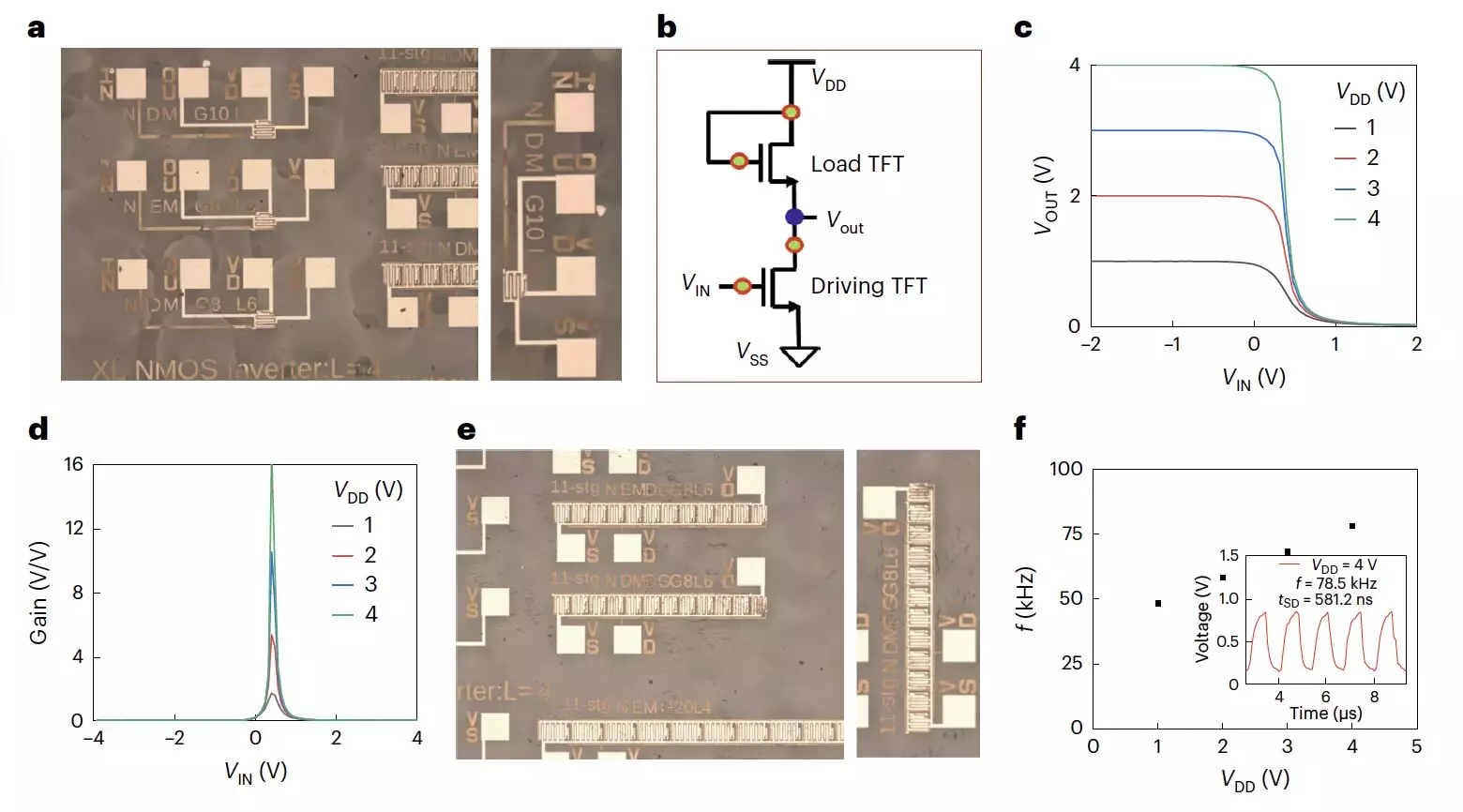
Initial tests of the n-type transistors designed by the researchers showed promising outcomes, including high electron mobilities, minimal hysteresis, and excellent operational stability under both negative and positive bias stress. The team has already utilized these transistors to create all-perovskite unipolar inverters and 11-stage ring oscillators, demonstrating the potential for integrated circuits with metal halide perovskite transistors. Moving forward, the proposed fabrication strategy opens doors for developing highly efficient and cost-effective electronics containing these innovative transistors.
The advancements in metal halide perovskite-based thin-film transistors represent a significant step towards the integration of these materials into modern electronics. With further research and development, the potential applications of these transistors in various electronic components are vast, paving the way for the next generation of high-performance integrated circuits.
Leave a Reply