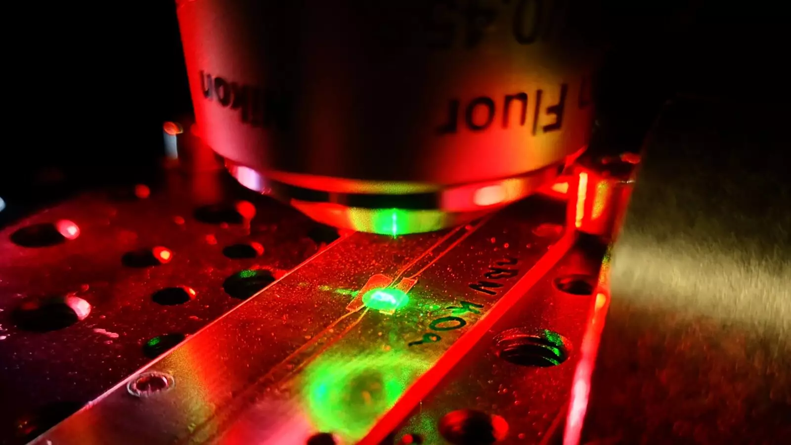
A recent breakthrough in quantum sensing technology has led to the development of a new 2D quantum sensing chip that is capable of detecting temperature anomalies and magnetic fields in any direction. This groundbreaking thin-film format chip, developed by researchers at TMOS and RMIT University, utilizes hexagonal boron nitride (hBN) to provide a more versatile and cost-effective alternative to current quantum sensors on the market.
In the past, quantum sensing chips have been predominantly made from diamond due to its robust nature. However, diamond-based sensors have limitations when it comes to detecting magnetic fields in various directions. These sensors can only detect magnetic fields when aligned in a specific direction, leading to blind spots when unaligned. As a result, diamond-based magnetometers require multiple sensors at different alignments, making them less versatile for different applications.
Advantages of hBN-based Sensors
The new quantum sensing platform developed by TMOS and RMIT University utilizes hBN crystals, which are flexible and can conform to the shape of the sample being studied. Unlike diamond sensors, hBN sensors can get much closer to the sample, allowing for more accurate and detailed readings. The unique defects in hBN produce different optical phenomena, with a recently discovered carbon-based defect capable of detecting magnetic fields in any direction.
Through careful experimentation and comparison with well-understood defects in hBN, researchers were able to determine that the new carbon-based defect behaves as a spin half system. This spin half nature allows the sensor to detect magnetic fields in any direction, providing a significant advantage over traditional diamond sensors. The researchers also found that this new defect can be controlled through electrical excitation, similar to existing sensors in hBN.
The development of this new 2D quantum sensing chip opens up a world of possibilities for a wide range of applications. One of the co-first authors, Sam Scholten, highlights the potential for using optically addressable spin defects in quantum materials to create nanoscale quantum sensors. The directional independence of the hBN sensor makes it ideal for applications in biological systems and other dynamic environments.
Future Research and Development
Looking ahead, researchers are eager to further explore the properties and opportunities presented by this new optical spin defect in hBN. By identifying and understanding the atomic defects in hBN, they aim to optimize sensor devices for superior performance. This research could lead to advancements in radio spectroscopy, magnetic field detection, and other areas where quantum sensing technology plays a crucial role.
The development of a new 2D quantum sensing chip using hBN represents a significant advancement in the field of quantum technology. This innovative technology has the potential to revolutionize magnetic field detection, opening up new possibilities for a wide range of applications across various industries. The future looks bright for quantum sensing technology, with ongoing research and development paving the way for even more groundbreaking discoveries.
Leave a Reply