In the world of semiconductors, the movement of electrical charges and their interactions with different materials are critical to advancing technology, particularly in the fields of energy harvesting and information technology. Researchers at UC Santa Barbara have made a groundbreaking leap by successfully capturing the first direct visual representation of electric charges as they traverse the interface of two semiconductor materials. This unprecedented breakthrough is expected to significantly deepen our understanding of charge transport processes, which have often been the subject of theoretical discussions but rarely observed directly in real-time.
At the heart of this research lies the concept of hot photocarriers, generated when photons—such as those from sunlight—excite electrons within semiconductor materials. Upon excitation, these electrons gain energy and begin to move, creating a flow of electric charge that can be harnessed for various applications, including solar panels and lasers. However, a fundamental limitation arises: a significant portion of the energy contained within these photocarriers dissipates as they transition to a cooler state within picoseconds (trillionths of a second). Understanding this loss of energy is crucial for improving the efficiency of photovoltaic systems, as it can directly influence their performance.
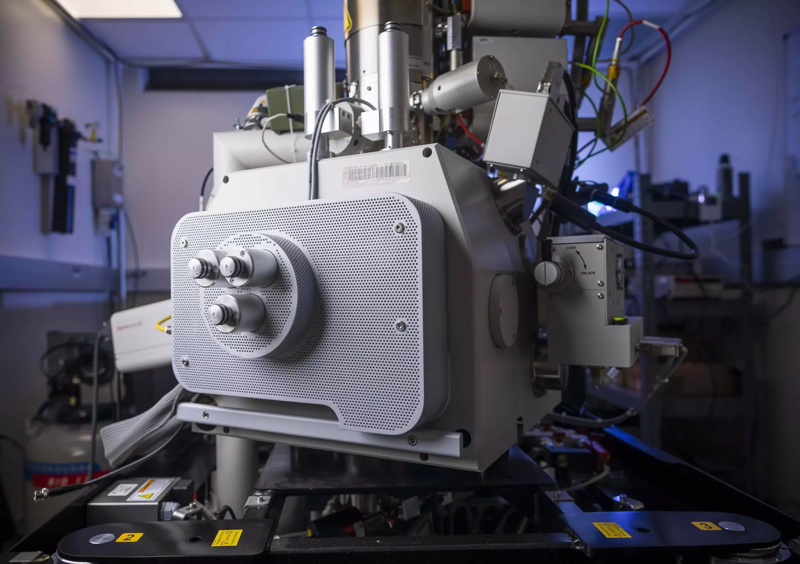
The research team, led by Professor Bolin Liao, utilized Cutting-edge scanning ultrafast electron microscopy (SUEM) techniques to visualize the elusive behavior of hot carriers in real-time. Characterized by very high spatial and temporal resolution, these techniques allowed the researchers to observe processes that occur on an incredibly quick timescale, providing insights previously thought to be inaccessible. Liao pointed out the value of direct observation compared to traditional theoretical or indirect measuring methods, stating, “There are a lot of textbooks written about this process from semiconductor theory. There are a lot of indirect measurements.”
Liao and his team specifically focused on the behavior of hot carriers within heterojunctions, or the interfaces formed between different semiconductor materials—specifically silicon and germanium in this case. Their innovative approach employed laser pulses to create a picosecond-scale shutter, enabling the capture of the fleeting movements of charged particles across the junction.
The stunning outcome of their research showcased how photocarriers diffuse across the boundaries of silicon and germanium, highlighting both the speed of their initial movement and the slowing effect induced by the junction potential. “If you excite charges in the uniform silicon or germanium regions, the hot carriers move very fast,” Liao emphasized. However, when charges are generated near the junction, some become trapped, resulting in significantly reduced mobility.
This discovery could lead to critical implications for semiconductor device design. The understanding that charge trapping at heterojunctions can adversely affect the efficiency of carriers could guide future efforts to create better-performing devices. Indeed, it is a striking confirmation of semiconductor theories long held in the academic community, showing the capability of SUEM to enhance researchers’ understanding of real-world semiconductor devices.
The outcomes of this research are poised to have broad implications across several areas of technology, including energy systems, telecommunications, and sensor development. By providing a clear picture of how hot photocarriers behave, scientists can better design semiconductor materials that maximize charge mobility and minimize energy loss, leading to more efficient devices.
Moreover, this research serves as a homage to the foundational concepts proposed by pioneering figures in semiconductor technology, such as Professor Herb Kroemer, who first suggested that the interface between materials is critical to device performance. More than just a confirmation of theory, this work has ushered in an era of enhanced capabilities in visualizing semiconductor processes, paving the way for future technological advancements.
The successful observation of hot photocarrier behavior marks a crucial milestone for semiconductor research at UC Santa Barbara. With the enhanced understanding of carrier dynamics and the ability to visualize these processes directly, researchers are armed with the tools necessary to push the boundaries of semiconductor technology further. As the field advances, we can anticipate a new wave of innovation, promising more efficient solar cells, refined electronic devices, and improved sensor technologies, ultimately contributing to a more sustainable and technologically adept future. The implications of this groundbreaking research extend beyond academic curiosity into practical applications that could reshape industries and enhance the way we harness energy and information.
Leave a Reply