Antiferromagnetic materials have captivated researchers due to their unique magnetic properties, which arise from the opposing orientations of neighboring atomic magnetic moments. Unlike ferromagnetic materials, which exhibit net magnetism, antiferromagnetic substances display zero net macroscopic magnetism, presenting intriguing possibilities for advancements in spintronic and electronic applications. Recent findings from Harvard University bring to light the antiferromagnetic diode effect observed in even-layered MnBi2Te4. This cutting-edge research has implications for next-generation devices, emphasizing the need for deeper understanding and exploration of antiferromagnetic phenomena.
Antiferromagnetic materials, by their nature, possess magnetic configurations where the magnetic moments of adjacent atoms are oriented in opposite directions. This configuration leads to a cancellation of the overall magnetic field, rendering these materials magnetically neutral on a macroscopic level. However, the manner in which these materials can manipulate electronic charge and spin opens new avenues in creating devices that rely on such properties. The Harvard team focused their research on MnBi2Te4, a material recognized not only for its antiferromagnetic characteristics but also for its centrosymmetric crystal structure, which traditionally does not favor the directional charge separation needed for diode functionality.
The implications of exploring these materials are substantial. Researchers envision applications in spintronic devices—where the spin of electrons is leveraged alongside their charge—enhancing efficiency and performance. Antiferromagnetic diodes could lead to improved performance in various electronic components, offering advantages like lower power consumption and increased durability.
The Harvard research team undertook a series of experiments to investigate the diode effect within even-layered MnBi2Te4. They constructed devices with two distinct types of electrode arrangements: Hall bar electrodes, which enable the precise measurement of hall-effect behaviors, and radially distributed electrodes arranged in a circular configuration. These designs allowed for comprehensive analysis of the antiferromagnetic diode effect, revealing nonlinear transport behaviors that underpinned their findings.
The experimental setup demonstrated that the anticipated diode characteristics could manifest even in the presence of a centrosymmetric configuration. This contradicts traditional notions regarding symmetry in diodes and highlights the potential of exploring new material classes that can yield surprising electronic behaviors.
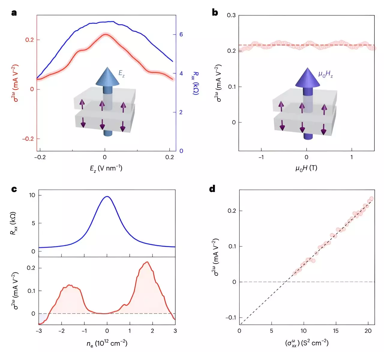
To validate and understand the antiferromagnetic diode effect, the researchers employed various sophisticated techniques. Among these was spatially resolved optical methods, which aided in visualizing the electronic behavior within the material. Additionally, they utilized electrical sum frequency generation (SFG) measurements to provide insights into the nonlinear responses exhibited by the material.
Gao, Chen, and their colleagues expressed excitement about their findings, noting significant second-harmonic transport in the devices, which is a hallmark of nonlinear electronic behavior. Their experimental results not only confirmed the presence of the antiferromagnetic diode effect but also illustrated potential applications in developing in-plane field-effect transistors and devices designed for microwave energy harvesting.
Implications for Future Technologies
The observed antiferromagnetic diode effect shines a light on the path forward for antiferromagnetic logic circuits, spintronic devices, and advanced microwave harvesting technologies. The researchers postulate that their work could act as a catalyst for subsequent investigations into antiferromagnetic materials and their electronic applications, potentially revolutionizing device architecture in the near future.
Given the rapid advances in materials science and electronic engineering, this research is pivotal in broadening the horizon for electronic device development. By exploring materials that deviate from traditional expectations, researchers can push the boundaries of what is deemed possible in semiconductor technology and beyond. The study not only embraces fundamental physics but also anticipates impactful real-world applications that may emerge from continued exploration of antiferromagnetic materials in electronics.
The Harvard team’s groundbreaking research on the antiferromagnetic diode effect in MnBi2Te4 marks a significant milestone in the quest for advanced electronic materials. Through persistent investigation and innovation, the potential for developing high-performance electronic components holistically intertwines with the principles of antiferromagnetism, paving the way for revolutionary changes in electronics.
Leave a Reply