Exploring the realm of two-dimensional materials unveils a world of unique properties and behaviors that differ from their bulk counterparts. When a material is thinned down to one or two layers of molecules, it undergoes a transformative process that leads to the emergence of novel characteristics. Research conducted by physicist Prof. Ursula Wurstbauer and her team from the University of Münster delves into the realm of two-dimensional crystals to understand how their properties can be manipulated to exhibit various behaviors such as being an insulator, electrical conductor, superconductor, or even a ferromagnet.
The key to unlocking the diverse properties of two-dimensional crystals lies in the interactions between the charge carriers, typically electrons, and the energy landscape of the crystals. By manipulating these interactions, the researchers were able to generate and quantitatively demonstrate collective excitations of the charge carriers within different energy landscapes. This groundbreaking study, recently published in Physical Review Letters, sheds light on the electronic characteristics of crystal structures and provides insights into ways to influence them.
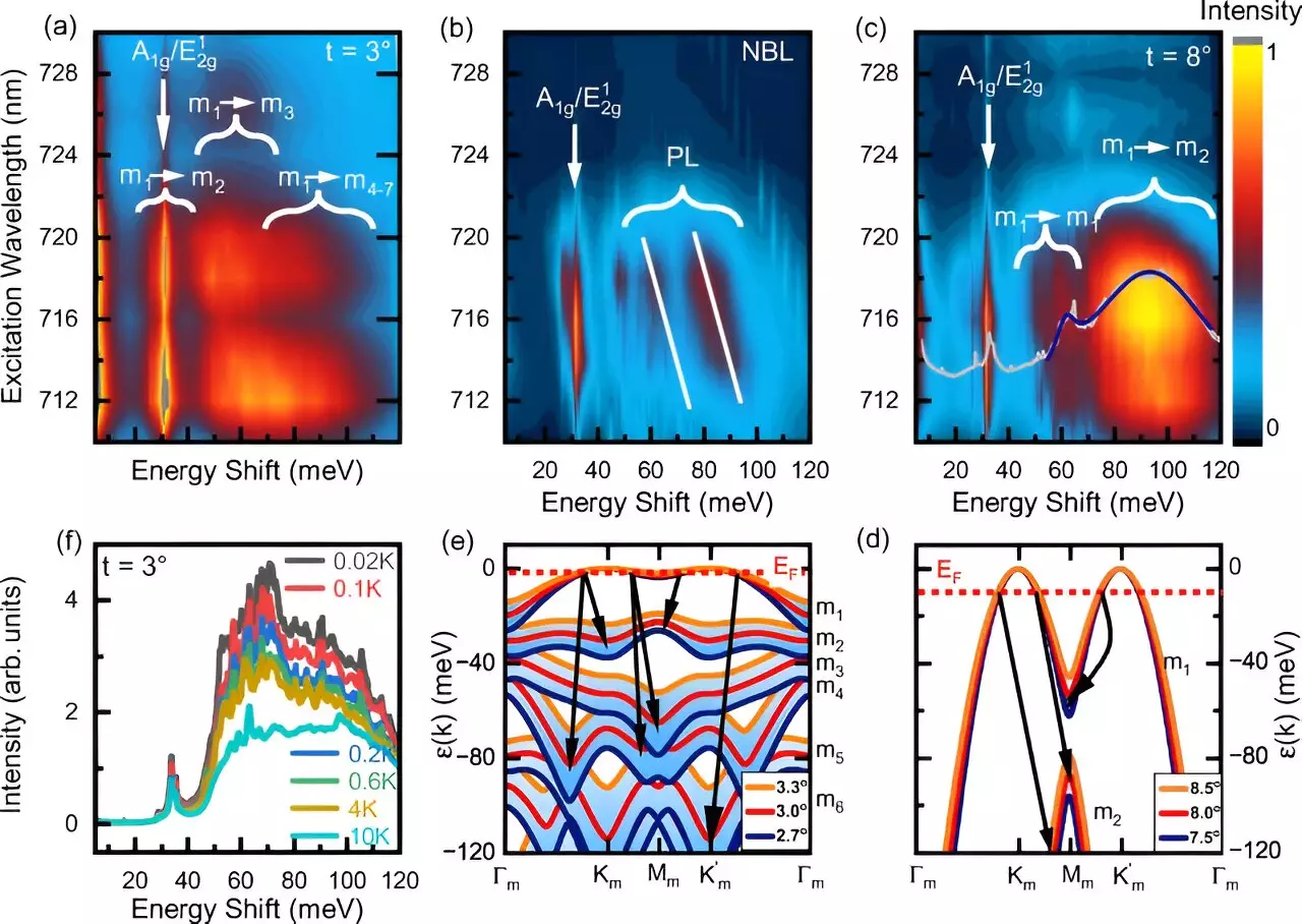
To achieve the desired properties, the scientists employed a technique of stacking two layers of a two-dimensional crystal and twisting them slightly against each other. This process creates geometric patterns known as moiré patterns, akin to thin curtain fabric layers laid on top of each other. These moiré patterns define the energy landscape and slow down the movement of electrons, leading to enhanced interactions among them. This phenomenon, termed strongly correlated behavior, results in electrons “feeling and seeing” each other and influencing their dance patterns within the crystal lattice.
The implications of these findings extend beyond fundamental research, with potential applications in quantum technology and the development of neuromorphic components and circuits. The intricate dance of electrons within two-dimensional crystals opens up avenues for innovative technologies that could revolutionize various fields. The collaborative efforts of the research team, which included scientists from the University of Hamburg, RWTH Aachen University, and the Max Planck Institute for the Structure and Dynamics of Matter in Hamburg, combined experimental work with theoretical analyses to unravel the mysteries of these material systems.
The researchers employed optical spectroscopy methods at cryogenic temperatures, specifically resonant inelastic light scattering spectroscopy, to analyze and characterize different two-dimensional crystals such as graphene, molybdenum diselenide, and tungsten diselenide. This multidisciplinary approach allowed them to gain insights into the complex behavior of electrons within these materials and pave the way for future advancements in the field of nanoscience.
The study of two-dimensional crystals presents a fascinating journey into the realm of nanomaterials with unique properties and potential applications. By understanding the interplay between charge carriers and the energy landscape of crystals, researchers can unlock a plethora of behaviors that hold promise for future technological innovations. The collaborative efforts of interdisciplinary research teams continue to push the boundaries of scientific understanding and pave the way for groundbreaking discoveries in the field of nanotechnology.
Leave a Reply