The development of two-dimensional (2D) semiconducting materials has opened up new possibilities for ultra-thin and tunable electronic components. Despite their promising potential, the challenge lies in effectively interfacing these materials with gate dielectrics without compromising performance.
Researchers at King Abdullah University of Science and Technology (KAUST), Soochow University, and other leading institutes have recently introduced a groundbreaking approach to improve the performance of transistors based on 2D semiconductors. By utilizing hexagonal boron nitride (h-BN) dielectrics and high cohesive energy metal gate electrodes, they have found a way to address the issue of interfacial traps that degrade transistor performance.
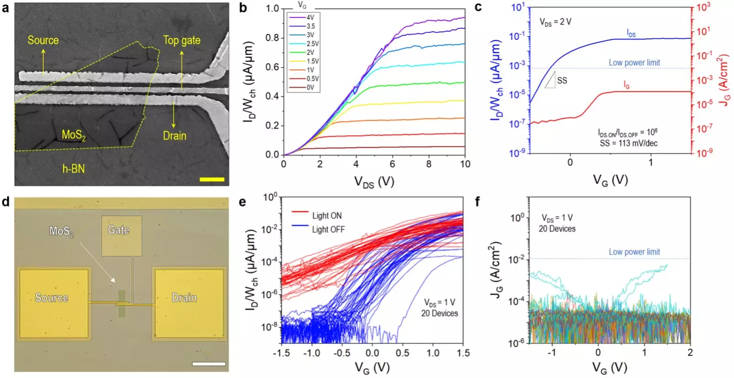
In their study published in Nature Electronics, the research team discovered that using platinum (Pt) as an anode in combination with h-BN stacks can significantly reduce dielectric breakdown. By fabricating over 1,000 devices with chemical vapor deposited h-BN as dielectrics, they demonstrated that Pt/h-BN gate stacks exhibit 500-times lower leakage current than Au/h-BN gate stacks, showcasing a high dielectric strength of at least 25 MV/cm.
The fabrication process involved cleaning a SiO2/Si substrate, patterning source and drain electrodes (Ti/Au), transferring MoS2 onto the electrodes to form the channel, and applying CVD h-BN film as the gate dielectric. Through electron beam lithography and e-beam evaporation, the team successfully created transistors with a vertical Pt/h-BN/MoS2 structure, establishing a clean van der Waals interface that enhances reliability and performance.
Contrary to previous beliefs, the researchers found that CVD h-BN can be an effective gate dielectric if paired with high cohesive energy metals like Pt and tungsten (W). The combination of MoS2 and h-BN forms a clean interface, reducing defects and improving gate control in field-effect transistors. This discovery paves the way for the use of 2D materials in solid-state microelectronic circuits and devices.
The team’s approach has shown promising results in reducing leakage currents and increasing the dielectric strength of 2D semiconductor-based transistors. Pt and W-based gate electrodes have demonstrated a significant reduction in leakage current compared to Au electrodes, setting the stage for the development of highly performing 2D semiconductor-based devices. This advancement could potentially lead to the extension of Moore’s Law through the development of ultra-small, fully 2D transistors.
With the success of this research, other research groups are likely to explore similar approaches and materials in the fabrication of 2D semiconductor-based devices. The continuous innovation in this field holds great promise for the future of electronic components and the advancement of technology as a whole. As we look ahead, the development of reliable 2D transistors could revolutionize the way we approach digital electronics and pave the way for new technological breakthroughs.
Leave a Reply