The field of electronics engineering is constantly evolving, with researchers and scientists striving to identify materials that can enhance the performance of electronic devices beyond the limitations of silicon-based transistors. One promising avenue of exploration is the use of two-dimensional (2D) semiconductors, which offer unique properties that could revolutionize the development of high-performance transistors.
While 2D semiconductors show great promise due to their atomically thin structure and high carrier mobilities, they also present challenges, such as high contact resistances caused by Fermi-level-pinning effects. These limitations can significantly impact the performance of transistors, hindering their integration into electronic devices.
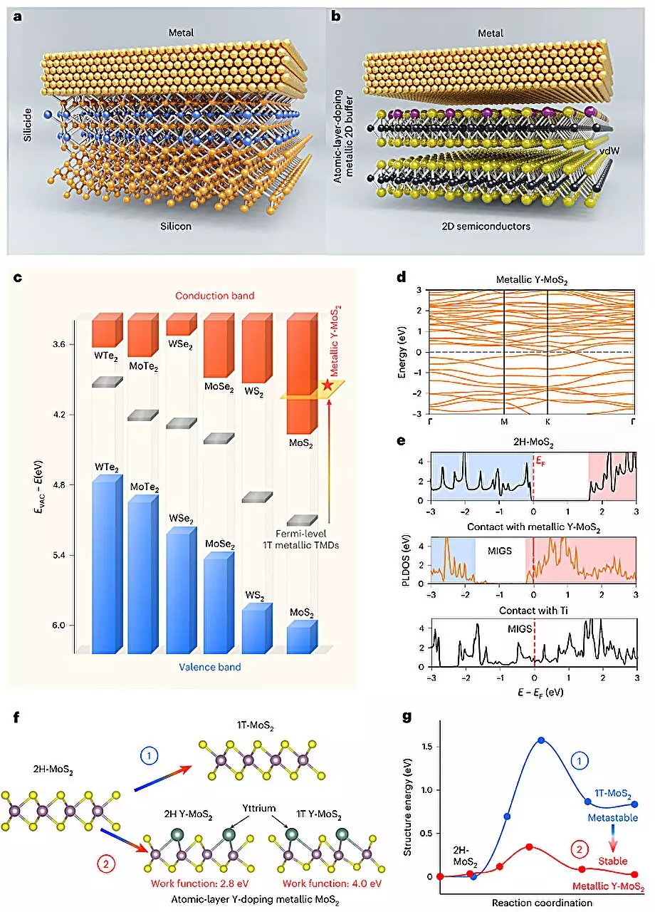
Recently, researchers at Peking University and Chinese Academy of Sciences have introduced a novel yttrium-doping strategy to address the issue of Fermi-level pinning effects in 2D semiconductors. By converting semiconducting molybdenum disulfide (MoS2) into metallic MoS2, the researchers were able to improve band alignment and facilitate the fabrication of ohmic contacts for 2D transistors.
To achieve yttrium doping in MoS2, the researchers developed the plasma-deposition-annealing (PDA) method. This involved treating patterned local contact areas with low-power plasma to create active sites, followed by the deposition of a Y/Ti/Au stacked metal, with the 1 nm-thick active metal Y serving as a solid-state doping source. Through high-temperature annealing in an inert gas environment, the Y atoms diffused into the material, leading to a phase transition to metallic MoS2.
The researchers introduced the concept of “rare earth element yttrium doping-induced 2D phase transition” in their study. This phase transition represents the metallization observed in MoS2 when subjected to the yttrium-doping strategy. By achieving a selective-area single-atomic-layer surface doping technique, the researchers were able to push the doping depth to the atomic layer limit of 0.5 nanometers, surpassing traditional engineering limitations.
Through their yttrium-doping strategy, the researchers were able to develop ultra-short MoS2-based channel ballistic transistors with excellent performance as ohmic contacts and impressive switching capabilities. These advancements pave the way for the development of new sub-1 nanometer node chips that offer remarkable performance while consuming less power than conventional chips. Additionally, the researchers aim to explore the development of equally effective p-type ohmic contacts for 2D semiconductors in the future.
The introduction of yttrium-doping in 2D semiconductors represents a significant breakthrough in the field of electronics, offering a pathway to overcome key limitations and enhance the performance of electronic devices. By addressing the challenge of contact resistances and achieving a phase transition to metallic MoS2, researchers have opened up new possibilities for the development of high-performance transistors and ultra-efficient electronic devices.
Leave a Reply